A Test IC for Wafer-Level Characterization of an IntraCMOS-MEMS Fabrication Process
Keywords:
Test devices, IC test, CMOS-MEMS, Integrated circuits, semiconductor devicesAbstract
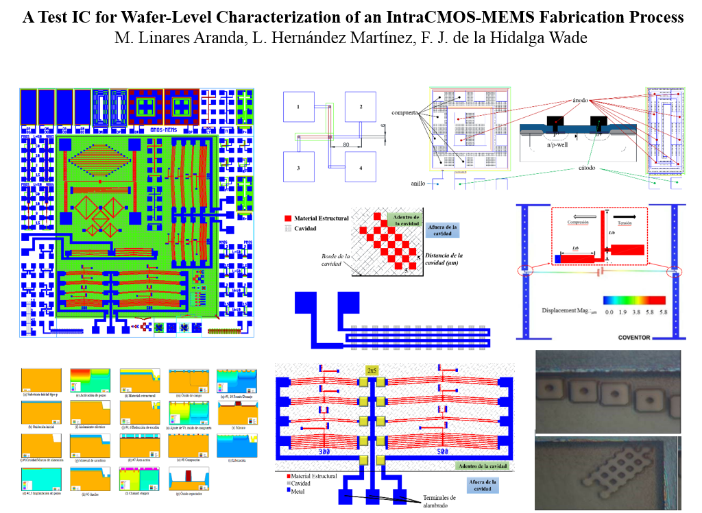
Monitoring of fabrication processes and the measurement of the electrical and mechanical properties of materials and devices at the silicon-wafer level are of vital importance on integrated system technologies. In this work, a test integrated circuit (IC) for the development of an IntraCMOS-MEMS fabrication process is presented. The test devices contained in the test IC are designed in such a way that 1) they can be used in CMOS-MEMS fabrication technologies using different materials, 2) take into account the capabilities of the manufacturing infrastructure, and 3) consider the selected integrated fabrication scheme; thus, any monolithic CMOS-MEMS process can be evaluated before, during and after the fabrication. The acquired data from the test devices will be useful to identify possible electrical and/or mechanical variations, in the properties of the materials used and in the performance characteristics of the devices, due to the fabrication process. The information acquired will help to adjust the simulation routines and the analytical modeling expressions. Finally, using the infrastructure of the MEMS Innovation Laboratory (LIMEMS-INAOE México) preliminary experimental results are presented.
Downloads
References
Sandia Lab’s. MEMS Video & Image Gallery, 2016. http://www.sandia.gov/mstc/mems_info/movie_gallery.html
P. H. Kao, P. J. Shih, C. L. Dai, and M. C. Liu, “Fabrication and characterization of CMOS-MEMS thermoelectric Micro Generators”, Sensors, vol. 10, no. 2, pp. 1315–25, 2010.
T. A. C. Fischer, F. Forsberg, M. Lapisa, S. J. Bleiker, G. Stemme, N. Roxhed and F. Niklaus. “Integrating MEMS and ICs” Microsystems & Nanoengineering, vol. 1, no. 1, pp. 1-16, 2015.
M. Bhushan and M. B. Ketchen, Microelectronic Test Structures for CMOS Technology, New York, Springer, 2011.
Y. Zhang, Y. Zhao, “An effective method of determining the residual stress gradients in a micro-cantilever”, Microsystem Technology, Vol. 12, no. 4, pp. 357–364, 2006.
C. A. Wilfrido, L. A. Mónico, T. J. Alfonso, B. Á. Carlos, “A Modular and Generic Monolithic Integrated MEMS Fabrication Process”, Revista Superficies y Vacío, Vol. 30, no. 3, pp. 30-39, 2017.
C. R. Báez Álvarez, “Diseño de un proceso integrado de fabricación de sistemas micro- electromecánicos (MEMS) genérico y modular”, Ph.D. thesis, Instituto Nacional de Astrofísica, Óptica y Electrónica, Junio 2016.
B. El-Kareh and R. J. Bombard, Introduction To VlSI Silicon Devices, Springer International Series in Engineering and Computer Science, 1986.
Y. B. Gianchandani, H. Kim, M. Shinn, “A fabrication process for integrating polysilicon microstructures with post-processed CMOS circuits”, J. Micromehanics and Microengineering, vol. 10, no. 10, 2000.
S. Beeby, G. Ensell, M. Kraft, N. White, MEMS mechanical sensors, Artech House, 2003. L. Elbrecht, U. Storm, R. Catanescu, and J. Binder, “Comparison of stress measurement techniques in surface micromachining”, J. Micromechanics Microengineering, vol. 7, no. 3, pp. 151-154, 1997.
L. Lin, A. P. Pisano, R. T. Howe, A micro strain gauge with mechanical amplifier, J. Microelectromechanical System, vol. 6, no. 4, pp. 313-321, 1997. F. J. Quiñones-N, F. J. De la Hidalga-W, M. Moreno, J. Molina, C. Zúñiga, and W. Calleja, “Mechanical characterization of polysilicon cantilevers using a thermo-mechanical test chip fabricated with a combined bulk/surface micromachining technique”, Results Phys., vol. 4, pp. 119-120, 2014.
T. M. Verhaar, J. Wei, and P. M. Sarro, “Pattern transfer on a vertical cavity sidewall”, J. Micromechanics Microengineering, vol. 19, no. 7, 2009.
C. R. Baez Alvarez, M. Linares Aranda, W. Calleja Arriaga, and J. Molina Reyes, “Effect of changing the material and device's properties on the performance of polysilicon-based Microactuators”, Int. Conf. on Electrical Engineering, Computing Science and Automatic Control, pp. 415-420, 2013.
M. G. Buehler, “Comprehensive test patterns with modular test structures: The 2 by N probe pad array approach”. Solid State Technology, vol. 10, pp. 89-94, 1979.