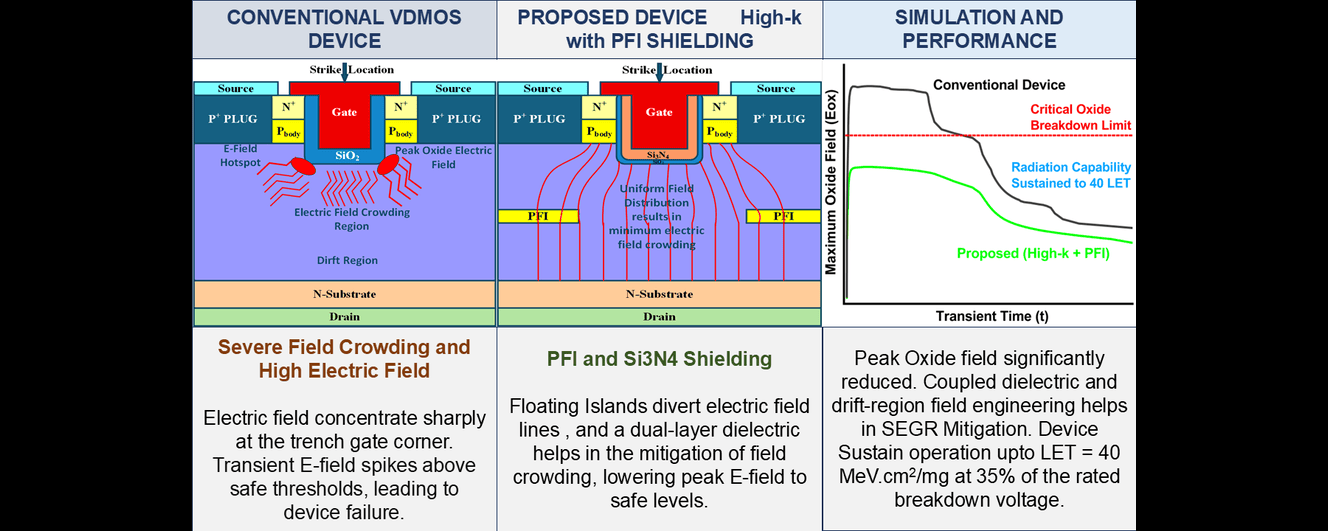
Electric Field Redistribution Driven SEGR Mitigation in a High-k Trench VDMOS with Floating Islands
Keywords:
Trench VDMOS, Single-Event Gate Rupture, high-k dielectric, floating islands, radiation effectsAbstract
Single-event gate rupture (SEGR) in trench-based power MOSFETs originates from transient oxide-normal electric fields generated during heavy-ion–induced charge transport, rather than from static breakdown limitations alone. Conventional mitigation approaches, such as stacked high-k gate dielectrics or drift-region field modulation using floating islands, address different aspects of the electric-field distribution but are typically examined independently. In this work, a TCAD-based study is presented to investigate how the co-integration of a high-k/SiO2 stacked trench dielectric and P-type floating islands in the drift region modifies electric-field partitioning under both steady-state blocking and transient heavy-ion irradiation. The combined effect of dielectric field redistribution and drift-region charge modulation reduces the peak oxide-normal electric field and delays the onset of gate rupture. Calibrated simulations indicate an increase in breakdown voltage relative to a conventional trench Vertical double-diffused MOSFETs (VDMOS) while maintaining comparable specific on-resistance. Under heavy-ion irradiation, the reduced oxide field enables sustained operation up to a linear energy transfer of 40 MeV · cm2/mg at 35% of the rated breakdown voltage. These results clarify the role of coupled dielectric and drift-region field engineering in SEGR mitigation and provide physics-based guidance for radiation-tolerant silicon power MOSFET design.
Downloads
References
B. J. Baliga, Advanced Power MOSFET Concepts. New York, NY, USA: Springer, 2010, doi: 10.1007/978-1-4419-6512-1.
J. L. Titus, L. S. Jamiolkowski, and C. F. Wheatley, Development of cosmic-ray-hardened power MOSFETs, IEEE Trans. Nucl. Sci., vol. 36, no. 6, pp. 23752382, Dec. 1989, doi: 10.1109/23.45451
A. Taber and E. Normand, Single-event upset in avionics, IEEE Trans. Nucl. Sci., vol. 40, no. 2, pp. 120126, Apr. 1993, doi: 10.1109/23.212327
P. G. Fuochi, Irradiation of power semiconductor devices by high-energy electrons: The Italian experience, Radiat. Phys. Chem., vol. 44, no. 4, pp. 431440, 1994, doi: 10.1016/0969-806X(94)90084-1.
G. H. Johnson, J. M. Palau, C. Dachs, K. F. Galloway, and R. D. Schrimpf, A review of techniques used for modeling single-event effects in power MOSFETs, IEEE Trans. Nucl. Sci., vol. 43, no. 2, pp. 546560, Apr. 1996,
doi: 10.1109/23.490900.
M. Allenspach et al., SEGR and SEB in n-channel power MOSFETs, IEEE Trans. Nucl. Sci., vol. 43, no. 6, pp. 29272931, Dec. 1996, doi:10.1109/23.556887.
J. L. Titus and C. F. Wheatley, Experimental studies of single-event gate rupture and burnout in vertical power MOSFETs, IEEE Trans. Nucl. Sci.,vol. 43, no. 2, pp. 533545, Apr. 1996, doi: 10.1109/23.490899.
S. Huang, G. A. J. Amaratunga, and F. Udrea, Analysis of SEB and SEGR in superjunction MOSFETs, IEEE Trans. Nucl. Sci., vol. 47, no.6, pp. 26402647, Dec. 2000, doi: 10.1109/23.903820.
J. L. Titus, An updated perspective of single-event gate rupture and single-event burnout in power MOSFETs, IEEE Trans. Nucl. Sci., vol. 60, no.3, pp. 19121928, Jun. 2013, doi: 10.1109/TNS.2013.2252194.
M. Allenspach et al., Single-event gate rupture in power MOSFETs: Prediction of breakdown biases and evaluation of oxide thickness dependence, IEEE Trans. Nucl. Sci., vol. 42, no. 6, pp. 19221927, Dec. 1995,
doi: 10.1109/23.489234.
K. Muthuseenu, H. J. Barnaby, A. Patadia, K. Holbert, and A. Privat, Ionizing radiation tolerance of stacked SiNSiO gate insulators for power MOSFETs, Microelectron. Reliab., vol. 104, p. 113554, Nov. 2020, doi:10.1016/j.microrel.2019.113554.
J. R. Cricchi and D. F. Barbe, Compensation of radiation effects by charge transport in metal nitride oxide semiconductor structures, Appl.Phys. Lett., vol. 19, no. 3, pp. 4951, Aug. 1971, doi: 10.1063/1.1653787.
V. A. K. Raparla et al., A model of radiation effects in nitrideoxide films for power MOSFET applications, Solid-State Electron., vol. 47, no. 5, pp. 775783, May 2003, doi: 10.1016/S0038-1101(02)00426-2.
S. M. Sze, Current transport and maximum dielectric strength of silicon nitride films, J. Appl. Phys., vol. 38, no. 7, pp. 29512956, Jun. 1967, doi:10.1063/1.1709881.
T. F. Wrobel, On heavy-ion-induced hard errors in dielectric structures, IEEE Trans. Nucl. Sci., vol. 34, no. 6, pp. 12621268, Dec. 1987, doi:10.1109/TNS.1987.4337463
T. P. Ma, Making silicon nitride film a viable gate dielectric, IEEE Trans. Electron Devices, vol. 45, no. 3, pp. 680690, Mar. 1998, doi:10.1109/16.661229.
R. Vaid and N. Padha, A novel trench-gate floating-island power MOSFET (TG-FLIMOSFET): A two-dimensional simulation study, Microelectron. Eng., vol. 88, no. 11, pp. 33163326, Nov. 2011, doi:
1016/j.mee.2011.07.013.
H.-C. Luo et al., Investigations of SiC VDMOSFET with floating-island structure based on TCAD, IEEE Trans. Electron Devices, vol. 66, no. 5, pp. 22952300, May 2019, doi:10.1109/TED.2019.2904370.
J. Zhang, L. Chen, and S. Yang, Investigation of SiC trench MOSFET with floating islands, IET Power Electron., vol. 9, no. 9, pp. 18681873, Jul. 2016, doi:10.1049/iet-pel.2015.0644.
D. Zhao et al., Novel step floating islands VDMOS with low specific on-resistance by TCAD simulation, Micromachines, vol. 13, no. 4, p.573, Apr. 2022, doi:10.3390/machines13040573.
H. Takaya, K. Miyagi, and K. Hamada, Improvement of floating island and thick bottom oxide trench-gate MOSFET, IET Power Electron., vol.4, no. 8, pp. 860866, 2011, doi:10.1049/iet-pel.2010.0205.
A. Galadi, F. Morancho, and M. M. Hassani, Breakdown voltage and on-resistance considerations in floating-island MOSFETs, Int. J. Electron., vol. 97, no. 3, pp. 241247, 2010, doi: 10.1080/00207210903292742.
S. Qingwen et al., Investigation of SiC trench MOSFET with floating islands, IET Power Electron., vol. 9, pp. 24922499, Oct. 2016, doi:10.1049/iet-pel.2016.0065.
K. Muthuseenu et al., Analysis of SEGR in silicon planar-gate super-junction power MOSFETs, IEEE Trans. Nucl. Sci., vol. 68, no. 5, pp.611616, May 2021, doi:10.1109/TNS.2021.3066625.
K. Muthuseenu et al., Single-event gate-rupture-hardened structure for high-voltage superjunction power MOSFETs, IEEE Trans. Electron Devices, vol. 68, no. 8, pp. 40044010, Aug. 2021, doi:
1109/TED.2021.3082756.
S. Krishnamurthy, R. Kannan, and F. A. Hussin, Single-event burnout hardening of trench-shielded power UMOSFET using high-k dielectrics, Mater. Res. Express, vol. 7, no. 3, p. 035907, 2020, doi:10.1088/2053-1591/ab6e6f.
X. Wan et al., SEB-hardened power MOSFETs with high-k dielectrics, IEEE Trans. Nucl. Sci., vol. 62, no. 6, pp. 28302836, Dec. 2015, doi:10.1109/TNS.2015.2495216.
R. K. Williams et al., The trench power MOSFET Part I: History, technology, and prospects, IEEE Trans. Electron Devices, vol. 64, no.3, pp. 674691, Mar. 2017, doi: 10.1109/TED.2017.2658340.
R. K. Williams et al., The trench power MOSFET Part II: Application-specific VDMOS, LDMOS, packaging, and reliability, IEEE Trans.Electron Devices, vol. 64, no. 3, pp. 692712, Mar. 2017, doi:10.1109/TED.2017.2658341.
Y. Wang, Y. Zhang, and C. Yu, Research of single-event burnout in power UMOSFETs, IEEE Trans. Electron Devices, vol. 60, no. 2, pp.887892, Feb. 2013, doi: 10.1109/TED.2012.2228905.
F. Morancho et al., A new generation of power lateral and vertical floating-island MOS structures, Microelectron. J., vol. 32, pp. 509516,May/Jun. 2001, doi: 10.1016/S0026-2692(01)00036-6.
A. Javanainen et al., SEGR in SiO2Si3N4 stacks, IEEE Trans.Nucl. Sci., vol. 61, no. 4, pp. 19021908, Aug. 2014, doi:10.1109/TNS.2014.2323952.
ATLAS Users Manual, Silvaco Inc., Santa Clara, CA, USA, 2016.
Silvaco, Single-event gate rupture simulations in a power MOSFET, Simul. Standard, vol. 23, no. 1, pp. 1012, 2013.
Z. Chen et al., Analysis and mitigation of single-event gate rupture in VDMOS with termination structure, IEEE Trans. Nucl. Sci., vol. 68, no.6, pp. 12721278, Jun. 2021, doi: 10.1109/TNS.2021.3077244.
Y. Zhang et al., A SEGR-hardened trench-gate DMOS with stepped source and optimized LOCOS structure, Microelectron. Reliab., vol. 162, p. 115525, 2024, doi: 10.1016/j.microrel.2024.115525.
X. Luo et al., Ultralow specific on-resistance superjunction vertical DMOS with high-k dielectric pillars, IEEE Electron Device Lett., vol. 33, no. 7, pp. 10421044, Jul. 2012, doi: 10.1109/TED.2012.2196969.
W. Saito et al., A 15.5 mΩ·cm2680 V superjunction MOSFET reduced on-resistance by lateral pitch narrowing, in Proc. IEEE ISPSD, 2006, pp.14, doi: 10.1109/ISPSD.2006.1666129.
Y. Lu et al., Design and simulation of a high-voltage double-trench MOSFET with ultra-low specific on-resistance, IEEE Trans.Electron Devices, vol. 68, no. 5, pp. 22182224, May 2021, doi:10.1109/TED.2021.3071174.
CoolMOS Power Transistor SPA15N60C3, Infineon Technologies AG, Neubiberg, Germany, Datasheet, 2003.
RF Power MOSFET ARF461A/BG, Microchip Technology Inc., Chandler, AZ, USA, Datasheet, 2008.